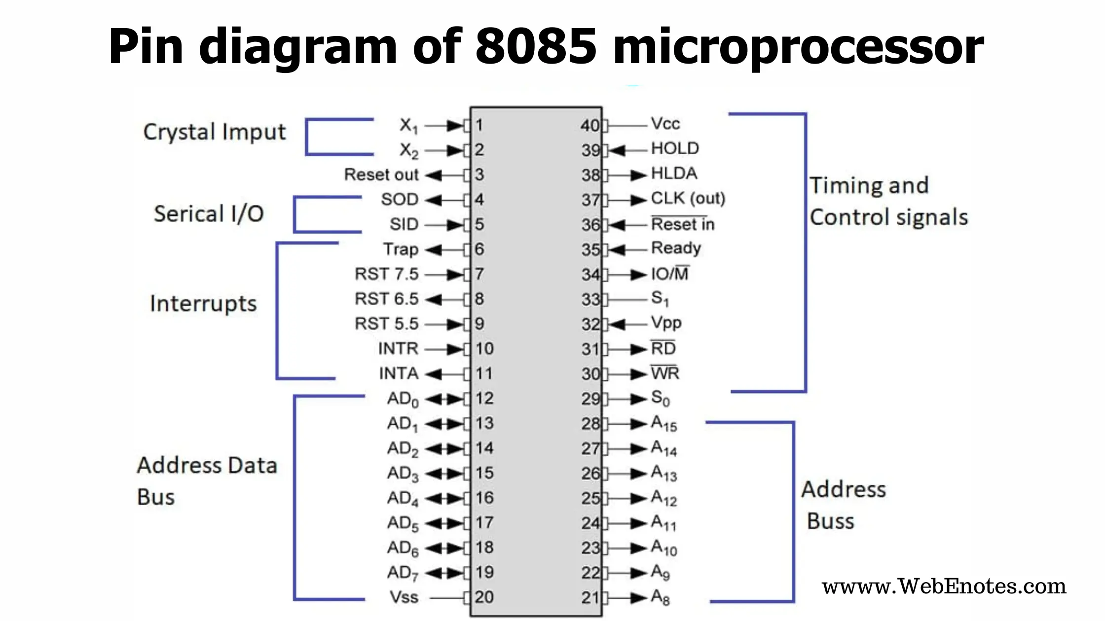
Pin diagram of the microprocessor 8085
It is 40 pin IC, DIP package. It works on a +5V single power supply. The figure is the pin diagram of the 8085 microprocessor.
Signals from the pins can be grouped as follows:
- Power supply and Clock Frequency signals
- Address bus
- Data bus
- control and status signals
- interrupts and DMA Request signals
- Serial I/O ports
- Reset signals
Pin diagram of 8085 microprocessor

- Power supply and Clock Frequency signals :
- Vcc +5 volt single power supply
- Vss Ground
- X1, X2: Crystal or RC network or LC network connections to set the frequency of the internal clock generator. The frequency is internally divided by 2 and used as the operating frequency. Since the basic operating timing frequency is 3 MHz, a 6 MHz crystal is connected externally.
- CLK OUT: It is an output signal, used as a system clock. The internal operating frequency is available on the CLK OUT pin.
2. Address bus:
- A8-A15: These are output, tristate signals used as higher order 8-bits of bit address.
- These signals are unidirectional meaning that the address is given by 5085 to select a memory or an I/O device.
3. Multiplexed address/data bus:
- ADO-AD7 These signals are I/O tristable signals.
- These pins provide multiplexed or time-shared addresses and data buses.
- The address is a lower order of the total 16-bit address i.e. A7 -A0. The bus works in conjunction with ALE.
- In the earlier part, it will output the address and will remain there for a finite time In the later part, it is as data but, i.e. either for reading or writing.
- But external peripherals requires separate address and data, therefore, to DEMULTIPLEX we use an external latch.
The Architecture Of Microprocessor 8085
4. Control and status signals
Control signals:
- The control signals of the 8085 microprocessor are IO/M(bar), RD(bar), WR(bar), and READY.
- IO/M(bar): Input-Output/Memory This is an output status signal, used to give information about operations to be performed with memory or an I/O device. When, IO/M 0, the microprocessor is performing a memory-related operation. and IO/M- 1, the microprocessor is performing an I/O device related operation.
- RD (bar)Read: This is an active low, output control signal used to read data from memory or an I/O device.
- WR: Write This is an active low, output control signal used to read data from memory or an I/O device.
- READY: This is an active high-input control signal. It is used by a microprocessor to detect whether a peripheral has completed the data transfer or not.
If it is HIGH, the up will complete the operation and proceed to the next operation. But if the READY pin is low, the microprocessor will WAIT.
Status signals:
- The status signals of the 8085 microprocessor are ALE, S0, and S1.
- ALE Address Latch Enable
This is an output signal used to give information on AD-AD, contents. When the ALE pulse is HIGH, it indicates that the contents of AD,-AD, are addressed.
When the ALE pulse is LOW, it indicates that the contents are data.

- S1 and S0: these are output status signals used to get information on the operation performed by the microprocessor.
Table: 8085 status signals
| S1 | S0 | Status |
| 0 | 0 | Halt |
| 0 | 1 | write |
| 1 | 0 | Read |
| 1 | 1 | Opcode Fetch |
5. Interrupts and DMA request signals Interrupt signals
Interrupt signals
- They are the signals initiated by an external device to request the microprocessor to do a particular task or work.
- There are five hardware interrupts and they are: TRAP RST 75> RST 6.5> RST 5.5> INTR.
- INTA(bar ): When INTR is active, the microprocessor generates an interrupt acknowledge signal INTA The INTA(bar) and INTR signals are basically used to expand the interrupt system to more than 5.
DMA request signals:
HOLD: It is an active high, input signal used by other controllers to request microprocessors about the use of address, data, and control buses. When the microprocessor receives the HOLD request signal, it completes the current machine cycle and will relinquish the use of the bus.
HLDA: The microprocessor in response to HOLD generates a signal that acknowledges the requesting device by HLDA signal When HLDA is active it indicates that the microprocessor has received the HOLD request and will relinquish the buses in the next clock cycle.
6. Serial I/O ports:
- SID: Serial input data. This is an active high, serial input port pin, used to access serial 1-bit data under software control.
- SOD: Serial output data. This is an active high, serial output port pin, used to transfer serial 1-bit data under software control
- These signals are used for serial communication.
7. Reset signals:
- RESET IN (bar): This is an active low, an input reset signal, When RESETIN(bar) =0, it clears the program counter i.e. 0000H, and address, data, and control lines tristate.
- RESET OUT: This is an active high, output signal used to indicate that microprocessor is reset. this signal is used as a system reset, to reset other devices connected to the system.
Also read,

